KiCad Symbol, Footprint and 3D Model Creation
Every time I need a component that is not in the official KiCad libraries, I create it from scratch. Over time I settled on a workflow that works well for me: symbol first, then footprint, then 3D model. This post documents that workflow so I can look it up when I need it.
This workflow targets KiCad 8.0.0 and later.
Symbol
The symbol represents the component in the schematic. I follow the KiCad Library Conventions (KLC) as a baseline for field names and layout.
The KLC defines a fixed set of standard fields. For a personal library I add two more fields to track sourcing information:
- MF: Manufacturer name, for example
Texas InstrumentsorKEMET - MPN: Exact manufacturer part number including package and Pb-free suffix, for example
C0402C103K3REC7411
Both fields are hidden on the schematic: uncheck the visibility checkbox when adding them.
For technical parameters that are useful to see directly on the schematic, I use two visible fields:
- Attr1: The first electrical parameter worth showing
- Attr2: The second electrical parameter worth showing
What goes into Attr1 and Attr2 depends on the component type:
| Type | Attr1 | Attr2 |
|---|---|---|
| Resistor | Tolerance (1%, 0.1%) |
Power rating (1/10W, 1/8W) |
| Capacitor | Voltage rating (50V, 25V) |
Dielectric (X7R, C0G, X5R) |
| Fuse | Current rating (2A, 10A) |
Blow characteristic (Fast, Slow) |
| TVS / protection | Clamping voltage (3.3V, 5V) |
Pulse power (400W) |
Four visible rows is the maximum that still looks clean on a schematic: Reference, Value, Attr1, and Attr2.
Additional attributes beyond Attr2 can be added as Attr3, Attr4, and so on, but they must be hidden since the 4-row limit is already filled.
If a second source exists for a component, MF2 and MPN2 can be added as optional hidden fields.
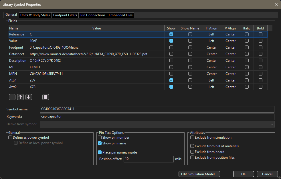 Symbol editor: a 10nF 0402 capacitor with all fields filled in
Footprint
The footprint defines the land pattern on the PCB. For most standard packages the official KiCad footprint library already has what I need. If not, I create one from the component datasheet.
Custom library files get a 0_ prefix in the filename.
This keeps them at the top of the list in the library browser and prevents name collisions with the official KiCad libraries. A custom 0_Capacitors.pretty will never shadow the official Capacitor_SMD.pretty.
I only consider a footprint complete once a 3D model is linked to it. No half-finished components in the library.
 Footprint editor with courtyard, fab layer, and 3D model already assigned
3D Model
A 3D model for every component makes it much easier to spot mechanical issues (connector clearances, component height violations, heatsink interference) before the boards are ordered.
I work through this priority list when looking for a model:
- Manufacturer-provided STEP file: Most manufacturers offer a
.stepfile on their product page or on Ultra Librarian or SnapEDA. - Community models: GrabCAD often has models for common components.
- Self-created in FreeCAD: For simple components where nothing is available, I model it myself.
Creating a model in FreeCAD
For simple components FreeCAD works well.
The kicadStepUpMod plugin handles coordinate alignment between FreeCAD and KiCad, so the model lands in the correct position without needing any manual offset or rotation in the footprint properties.
The plugin exports both .step and .wrl in one step.
As of KiCad 6, the 3D viewer renders
.stepfiles directly. The.wrlformat is no longer required by the KLC and can be omitted for personal libraries.
The finished model should sit on the footprint correctly with all rotation and offset fields at zero in the footprint properties. If values are needed there, the model is not properly aligned and should be corrected in FreeCAD before committing it to the library.
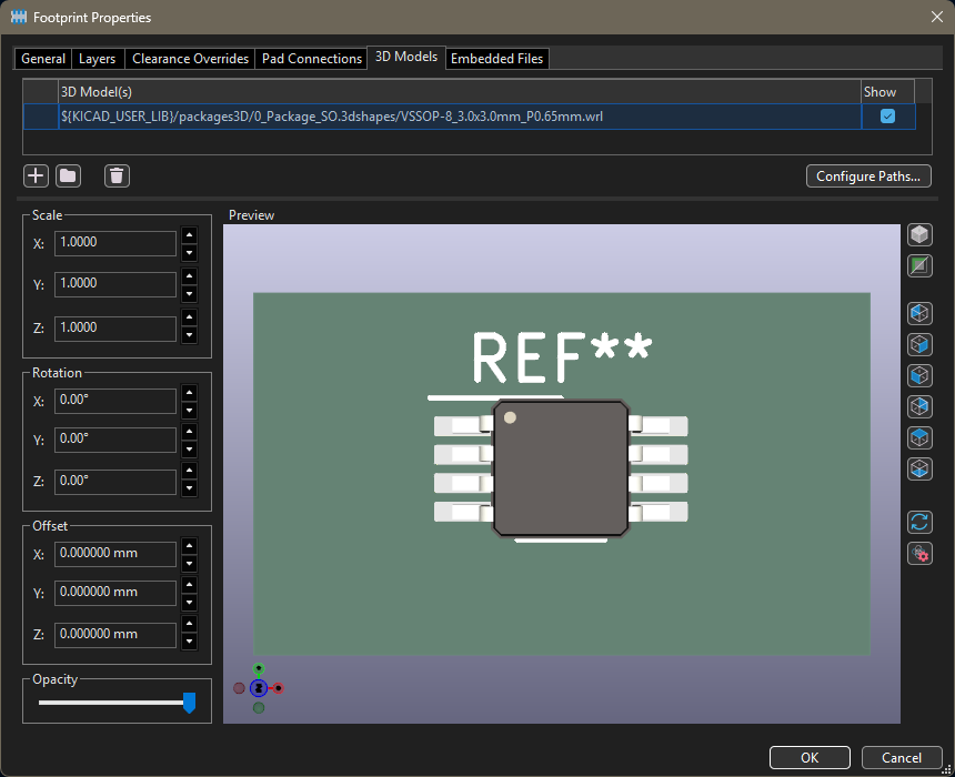 Finished component in the KiCad 3D viewer, no manual offset needed
Adding the Library to KiCad
I use the library globally, so it only needs to be set up once and is available in every project.
Symbol libraries: Open Preferences > Manage Symbol Libraries, switch to the Global Libraries tab, and add each .kicad_sym file from the symbols/ directory.
Footprint libraries: Open Preferences > Manage Footprint Libraries, switch to the Global Libraries tab, and add each .pretty directory from the footprints/ directory.
For the library path I use a custom environment variable KICAD_USER_LIB that points to the root of the library repository.
This keeps all paths short and makes it easy to move the library to a different location without having to update every entry.
The variable is set under Preferences > Configure Paths.
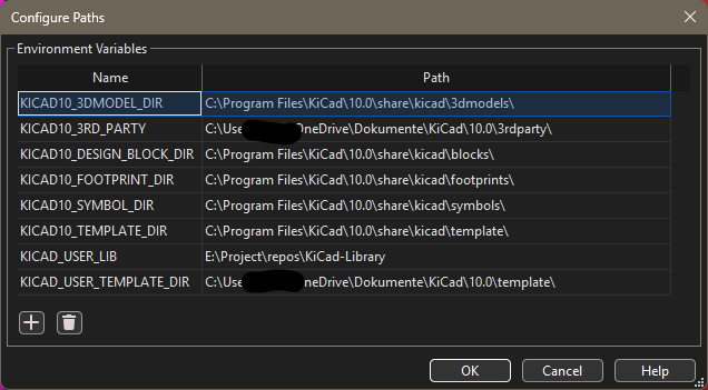 Custom path variable in KiCad pointing to the library root